


(Non)Announcement of a Milestone in 1.8nm Production
Is Intel on track to overcome its long crisis? It will be decided by company’s fabs – a strategic advantage but now a burden the company can no longer afford. Intel now needs external clients to sustain them and whether these clients will come depends on the ability to deliver competitive technologies. The company is pinning its hopes on the 18A process. Production using this technology has just begun, so the answer may come soon.
The announcement was made in an unusual way—one of Intel’s executives, an engineering manager named Pankaj Marria, posted on LinkedIn stating that wafer production using Intel’s 18A technology has been launched at the company’s Arizona facility. 18A means 18 ångströms, so Intel is effectively calling the technology a 1.8nm process, although such designation is not used by the company.
The engineer mentioned that the process is being rolled out by the “Eagle Team”, symbolically named to reflect the importance of the 18A process (and Intel’s renewed ability to manufacture using the most advanced processes) has for the self-sufficiency of the U.S. technology industry. To mark the occasion of the “first batches” of 1.8nm wafers, the team reportedly printed posters with the slogan The Eagle Has Landed (a reference to the announcement of the Moon landing).
However, the photos and the LinkedIn post were later deleted, which is also somewhat remarkable. Perhaps higher-ups did not want such announcements to come from lower-level employees, or the company, in the interim period just before the arrival of the new CEO, wass unsure how much to promote this technology (although it doesn’t seems likely that Lip-Bu Tan could yet scrap the production plans).
It’s worth noting that this production kick-off should not mean that it is only now that Intel is getting their very first 1.8nm chips. Intel has already had samples of Panther Lake processors for some time, and it’s quite possible that samples of chips being tested by external customers also exist. However, these chips were likely made on a separate line used for process development. The significance of the deleted post from the Arizona team lies in the fact that this technology has now apparently been installed and activated in the Fab 52 and Fab 62 facilities, where mass production for commercial purposes will take place, including Panther Lake processors (Core Ultra 300) from Intel. These are expected to launch in the second half of the year.
The 18A process
The 18A technology will be the first to introduce GAAFET transistors using nanosheets (Intel calls them RibbonFET) instead of FinFETs. Simultaneously, this process generation will debut the PowerVIA technology, a form of backside power delivery (explained in detail in this article). This approach separates the power delivery wiring from the logic and circuit wiring in the traditional metal layers of the chip.
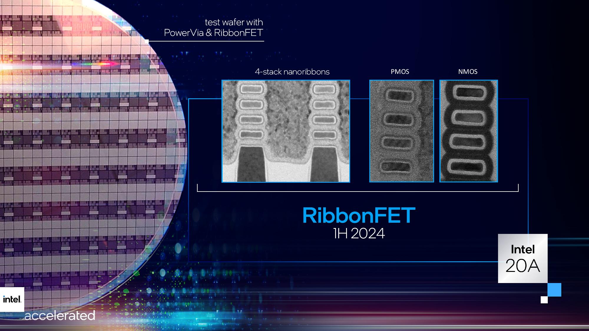
Instead, additional metal layers for power delivery are created on the backside of the chip. This is an extremely demanding change to the entire chip manufacturing process and design, given how wafers are processed and chips manufactured. However, this change should enable improved transistor density, as eliminating power delivery wiring in the traditional BEOL of the chip allows for tighter packing of logic circuits in the metal layers. We’ve written more about Intel’s planned processes here:
- Tip: Intel Unveils Manufacturing Process Roadmap: 7 nm to 18 A, RibbonFET
- Tip: Intel’s Manufacturing Process Roadmap: Tick-Tock, 2 nm, and 1.8 nm by 2024
- Tip: Intel announces 1.4nm process, first node with high-NA technology
The Intel 18A process may not yet fully match the technology state of the art achieved at the time by TSMC – the Taiwanese leader will likely have its 2nm technology ready or almost ready by the time Intel’s 1.8nm chips hit the market. Despite the nominally smaller “number,” TSMC’s technology is likely at least slightly ahead of Intel’s 1.8nm process, with Intel’s 18A perhaps being more comparable to TSMC’s 3nm process (N3). This is suggested, for example, by Intel’s decision to use TSMC’s 2nm process for its Nova Lake processors, while the previous generation, Panther Lake, will utilize the Intel 18A process. This indicates which process is seen as the more advanced one.
Chips from Nvidia, Broadcom?
The biggest question is how successful the process will be among external customers. According to a Reuters report from earlier this month, companies including Nvidia and Broadcom are considering using the 18A process, with both firms already producing test chip samples at Intel.
However, for now, these are reportedly just non-product test chips, not samples of products directly intended for later mass production. Any large-scale orders from these companies can therefore only start much later (because once these companies determine that the technology is viable, any real product will need to go through roughly a year-long cycle from tape-out, from that point). It was also announced some time ago that Microsoft plans to manufacture some of its own chips using Intel 18A process, though it’s unclear if this plan is still in place.
Sources: Tom’s Hardware, Reuters
English translation and edit by Jozef Dudáš
⠀


