

Intel's processor designed for maximum power efficiency unveiled at Computex
Intel has unveiled the Lunar Lake processors at Computex, said to be the most mobility and efficient CPUs (allegedly the best in the x86 world) and compete against Apple chips as well as against other ARM processors in Copilot+ PCs, in addition to facing AMD. And it’s much more than just the P-Core and E-Core architectures, Lunar Lake basically combines the best technologies Intel has to across various fields into a single package.
Lunar Lake has eight cores, four big P-Cores with Lion Cove architecture (without HT) and four little and efficient Skymont E-Cores, and is a chiplet-based (tile-based) processor like the previous generation Meteor Lake. In addition, it features a new integrated GPU with 1024 shaders. And a powerful next-generation NPU is also integrated.
Intel Inside… Made in TSMC
But Lunar Lake uses fewer active chiplets – only two instead of four, the Compute and SoC Tile (known also as the Platform Controller Tile, as this die has a similar function to the existing chipsets known as PCH, Platform Controller Hub). These chiplets lie on a passive interposer base tile. The compute chiplet will be manufactured on TSMC’s 3nm N3B node, like Apple’s M3. This will be the first 3nm x86 processor.
The SoC chiplet uses TSMC’s 6nm node. So Lunar Lake is a processor manufactured virtually completely outside of Intel’s foundries, a previously unheard of thing given how Intel relying on their own fabs used to be seen as a critical advantage for the company. Intel’s manufacturing lines only perform advanced packaging of TSMC-made silicon, using Foveros technology. Note that the passive interconnect base chiplet is actually made with Intel’s old 22FFL technology, but this is a pretty unremarkable and incomplicated part of the whole processor.

Lunar Lake uses on-package memory, which means LPDDR5X packages soldered directly to the CPU package instead of the motherboard. While it’s not actually any sort of advanced packaging technology (unlike say HBM or other 2.5D and 3D packaging technologies), the shorter wire path allows you to use lower voltages and in some cases get away with not using termination. It is the same solution that Apple uses for the M-series processors.
This solution reduces power consumption (but not performance, which is something widely but incorrectly reported with regards to Apple’s processors). According to leaks, memory capacity will vary by model number. For example, the same Lunar Lake processor will be called Core Ultra 5 238V with 32GB of integrated memory and Core Ultra 5 234V with 16GB of memory.
- Tip: Intel’s new P-Core: Lion Cove is the biggest change since Nehalem
- Tip: Skymont architecture analysed: Intel little core outgrows the big?
Remarkable new CPU architectures
Lunar Lake has very interesting new CPU cores, in the case of both the big P-Core (Lion Cove) and the little E-Core architectures. We have covered these in separate articles, which we bring to your attention, here it is enough to mention that the so-called little cores in Lunar Lake should have 2% better IPC (or performance per 1 MHz) than the previous big cores in Raptor Lake processors (but probably significantly lower clock speed) and the big cores should have 16% higher IPC than the Redwood Cove core in Meteor Lake processors (which itself should have the same or slightly worse IPC as Raptor Lake).
Redesigned Low Power Island and improved Thread Director
Little cores, or rather E-Cores (Skymont is far from a small core architecturally, although its area is probably much smaller than the very large “Cove” cores) have undergone an important change. Intel used to place them on the ring bus and the L3 cache of the processor, which had a negative effect on the power consumption during their operation.
In Meteor Lake, Intel has placed some of the cores outside of the Compute chiplet, on the SoC chiplet. There were only two of these cores and they were supposed to run low-demand background loads or video playback for example, but it seems that in Meteor Lake this didn’t have as beneficial an effect as expected, perhaps due to the lack of performance of the only two cores (with low clock speed).

In Lunar Lake, all the E-Core cores are back on the Compute chiplet, which is now also the home of the Low Power Island. This includes all four E-Cores, which are all removed from the L3 cache (they only use their L2 cache) and the ring bus of the big cores. Thus, when running, the processor typically shuts down the entire ring bus and L3 cache when not experiencing high loads, to save power. And opportunistically, it probably shuts down even the SoC chiplet functions as well, keeping just the low-power island part of the Compute Tile on.

For Lunar Lake, the next generation of Intel Director technology in Windows 11 will be deployed to better control the workload distribution between E-Cores and P-Cores. The new version is intertwined with power management, gives better feedback to Windows and is further optimized.
In default mode,when scheduling tasks, the E-Cores in the Low Power Island will be preferred as the first choice. The system will try to do all the work on these cores, initially on a single E-Core, as long as the performance is sufficient. Only at heavier workloads will it activate more E-Cores until it detects that the application is so demanding that it needs a P-Core or all cores (for multi-threaded applications). However, a single P-Core alone can probably be activated for single-threaded programs if the system assesses that they need the maximum 1T performance (benchmarks like SuperPi, audio encoding, etc.).

According to Intel, most real-world programs and workloads should remain resident within the Low Power Island most of the time, including applications using multiple threads, so Lunar Lake should ordinarily be running with all four E-Cores active while all four P-Cores are still suspended. This will be the case, for example, with the Teams application that Intel used for the Lunar Lake efficiency demos. Teams does use four cores, but it stays purely on E-Cores, and this reduces power consumption during video conferencing by up to 35%. But it’s possible that this also depends on the cooperation of the application’s author, Microsoft may have optimized the program specifically to behave like this on the Lunar Lake platform.
SLC Cache
While Low Power Island and E-Cores do not have access to the L3 cache of large cores, they benefit from the so-called SLC (System Level Cache, do not confuse with SLC NAND). This is something like the L4 cache, but it serves not only the CPU cores, but also other blocks in the processor, such as the NPU, GPU, multimedia block.
Its capacity is 8 MB and should probably be attached to the memory controller. The SLC is intended to keep some working data directly in the processor to reduce power-consuming data transfers from RAM. SLC is a component that has long been used for these purposes in ARM processors, for example in mobile phones, and in Lunar Lake it should extend the battery life of a computer similar to how it benefits the mobile phone SoCs.
New NPU and 1.5x faster Battlemage graphics with XMX
The NPU of Lunar Lake processors features a new architecture (NPU 4) compared to that of Meteor Lake processors. NPU 4 contains 3× more matrix blocks (12,000 in 6 NCE blocks), has 12× more powerful SHAVE vector units than the NPU 3 in Meteor Lake, and supports INT8 (2048 MAC operations per cycle) and FP16 operations (at half-performance compared to INT8 though, 1024 FMAC operations per cycle). This architecture is claimed to achieve 2x better power efficiency.

Overall, it delivers 48 TOPS in INT8 operations, slightly more than the 45 TOPS of the Qualcomm Snapdragon X Elite and slightly less than the 50 TOPS of the AMD Ryzen AI 300. However, the differences are small and application performance will probably vary more as a result of different architectures (and possibly also the quality of the software support) than strictly based on the given TOPS numbers. Microsoft has set 40 TOPS as the threshold for using Copilot+ PC features, which these three processors all meet.
An additional 67 TOPS of performance in INT8for AI applications can be provided by the integrated GPU, which has a new Xe2 LPG architecture which is derived from the upcoming second-generation Intel Arc standalone GPUs (Battlemage). In comparison Meteor Lake (and also Arrow Lake) use older generation Xe LPG architecture coming from Alchemist GPUs.
The GPUs include XMX matrix units for AI acceleration, which are present in the Arc Alchemist graphics architecture, but the derivative mobile Xe LPG variant integrated in Meteor Lake lacked them. That 67 TOPS performance in AI is thanks to the XMX units.

This GPU has 1024 shaders, 128 XMX units, 8 RTUs (ray tracing accerators) and a large 8MB L2 cache that should improve performance with shared RAM, which is usually a sore point for integrated GPUs.

In general, this integrated GPU is said to be 50% more powerful in gaming and graphics applications compared to the also quite capable Meteor Lake GPU, which also had 1024 shaders. The question is whether this is just peak performance, or if there will also be +50 % uplift in sustainable level of performance when gaming with the low TDP of Lunar Lake processors.
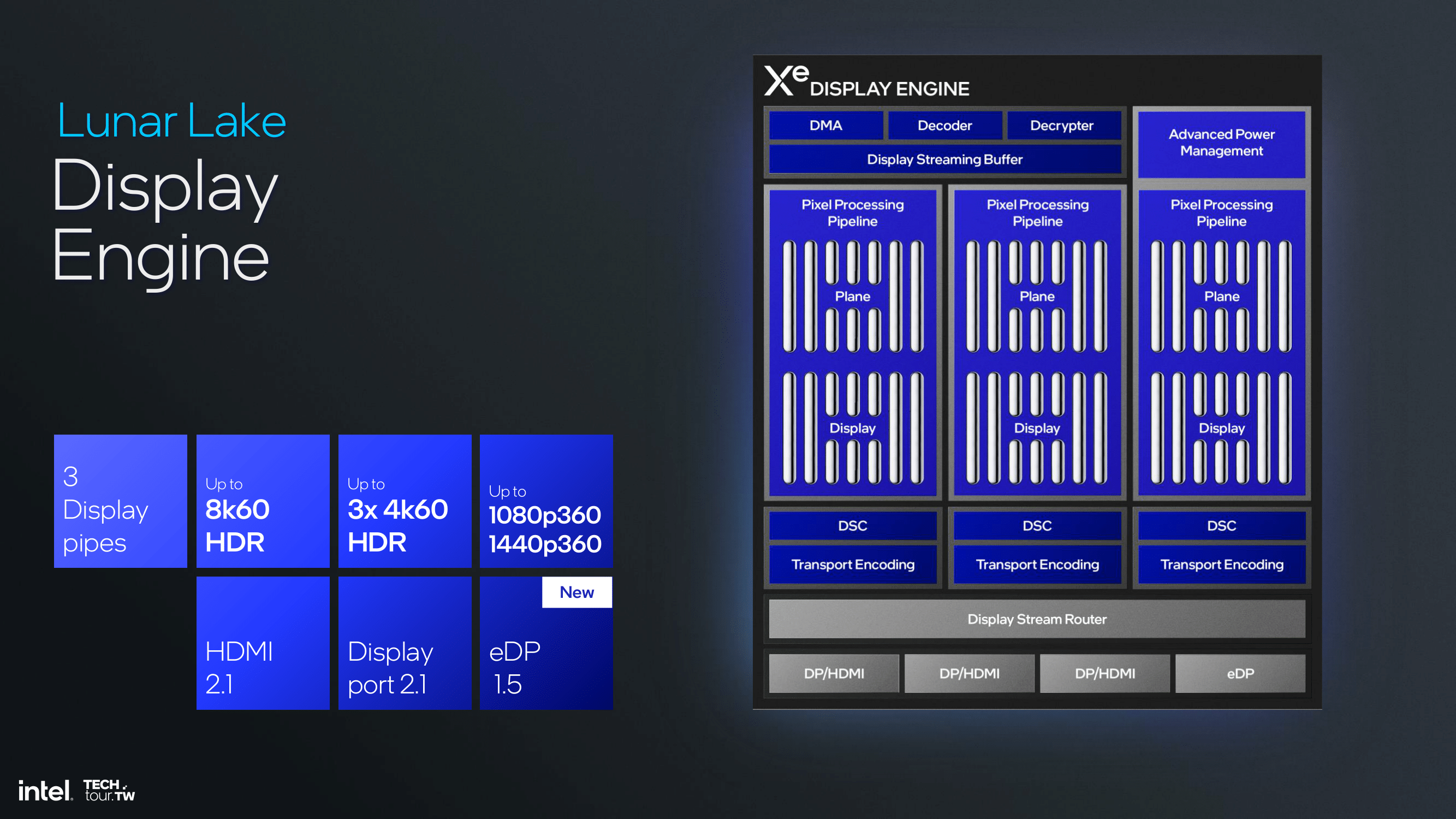
DisplayPort 2.1 and VVC format video support
In addition to the Xe2 LPG / Battlemage architecture, the Lunar Lake processor has a new display output block with support for HDMI 2.1, DisplayPort 2.1 and eDP 1.5. It can handle three 4K monitors at 60Hz with HDR simultaneously, or one 8K display with HDR at 60Hz. In gaming devices, it can support 360Hz displays at 1080p or 1440p.
Also new is the multimedia block, where the most interesting improvement is the addition of hardware decoding of the compression format VVC alias H.266, a new format from MPEG and ITU, the authors of the HEVC standard, which should be of higher quality than AV1 developed mainly by Google and Netflix. Intel claims that VVC can provide the same quality with roughly 10% less file size or bitrate.

Intel is expected to be the first to market with VVC support with Lunar Lake (at least when we are looking at various PC processors). Besides VVC decoding, the multimedia block supports compression and playback of other formats with up to 8K resolution, as well as resolution switching in video on the fly, for example in adaptive streaming.
Thunderbolt and Wi-Fi 7
PCs with Lunar Lake will probably often combine video output with Thunderbolt connectivity in USB-C ports, as there is a Thunderbolt 4 controller integrated directly into the processor, providing up to three 40Gbps ports.

Thunderbolt Share technology will also be supported.
For the first time ever, Lunar Lake also has integrated Wi-Fi 7 (and Bluetooth 5.4) wireless connectivity, the digital part of which is present directly in the SoC chiplet, but as usual you will need to connect an external radio part via the CNVi interface. The usefulness of this will therefore be tied to the use of Intel’s CNVi module (Intel BE201).

PCIe 5.0
The SoC chiplet also provides USB 2.0 and 3.0 connectivity for common non-Thunderbolt ports, but here’s a surprise: It also provides a PCIe 5.0 controller, which we did not expect in a processor optimized for power consumption.

So when any PCIe 5.0 SSDs come to market that have better power efficiency than PCIe 4.0 modules, Lunar Lake will be ready for them (competing Snapdragon X Elite or AMD Ryzen AI 300 can only do PCIe 4.0, although we do not consider this to be a significant issue). It’s possible that this support will be usable with Samsung SSD 990 Evo modules, for example.
The SoC chipset also provides PCI Express 4.0 lanes, but we don’t have information on the exact number yet. The lanes will be optimized to connect a single SSD and possibly for wireless connectivity. It is quite likely that the processor will not have a larger number of lanes for the eventual GPUs. And if it does, it will probably only have maybe four lanes.
Release will be in Q3
According to Intel, the release of these processors is supposed to occur in the third quarter, at Computex 2024 Intel has for now only presented its architectural details and integrated features. However, the company has not yet disclosed anything about the specific SKUs and other specifications of these processors (like clocks, TDPs), so it remains unclear how high the performance will be.
These specs will determine whether the processor will excel only in efficiency or also have the performance to compete with the fastest mobile CPUs of today, such as the aforementioned Snapdragon X Elite, Apple M3 and M4 or AMD’s Ryzen AI 300 and Ryzen 9000.

The final launch is expected to take place in the third quarter of the year. Earlier, there were reports that laptops with these processors could apparently only hit the market in the fourth quarter, but Intel is talking about availability starting in the third quarter now, so they could be here as early as August or September.
You can expect models from about all manufacturers (Intel lists 20 partners and 80 models), with the notebooky often being Copilot+ PCs with Microsoft’s AI features in Windows 11.
Sources: Intel, AnandTech, Tom’s Hardware
English translation and edit by Jozef Dudáš
⠀