


Nvidia's new 4nm GPU generation is here
It’s been roughly two years since Nvidia has unveiled its 7 nm Ampere compute GPU (the A100 accelerator). Now the company is introducing a successor – the new Hopper GPU architecture and with it the Nvidia H100 compute GPU, which is based on a die called GH100. This is the most advanced and powerful GPU yet, manufactured for the first time on the 4nm process. But it also has the dubious honour of being the most power-hungry GPU ever.
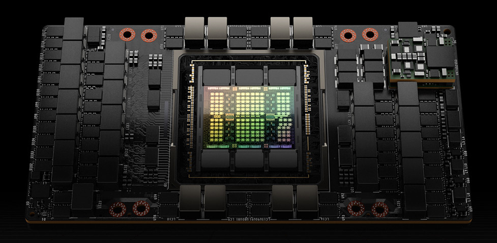
GH100 chip
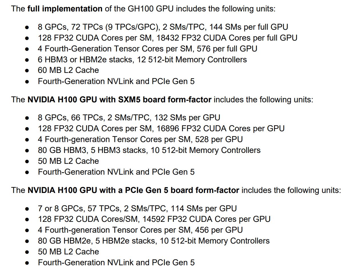
The Nvidia H100 accelerator (which is a descendant on the earlier Tesla line, but that brand is no longer used by Nvidia) is again a server-specific GPU that is not intended for gaming. The fully enabled version of the chip is made up of 8 GPC blocks, each containing 9 TPC sub-blocks, which in turn consist of two SM blocks of 128 shaders or stream processors each (or “Cuda cores” as Nvidia calls them, however these are not separate cores, they are much closer to SIMD lanes).
In total, this is 144 SM blocks and 18,432 shaders in them, the highest number a GPU-based accelerator has packed so far. This is logical, of course, as the GH100 is the first chip from the new generation of 5 nm/4 nm GPUs. Each SM block again contains four Tensor Core units to accelerate matrix operations used by neural networks (a.k.a. artificial intelligence). This field will again probably be the most important deployment target of these GPUs. So a fully active GH100 chip would have 576 tensor cores. It does not, on the other hand, contain any RT cores for ray tracing acceleration.
Generally, the H100/Hopper probably won’t even support graphics fixed function operations at all, although there has been some unconfirmed information (a hint found in data recently stolen by hackers from Nvidia) that support for graphics computing could supposedly be retained in a single GPC block, so the chip would have basic compatibility with 3D graphics. We’ll see if this capability is confirmed and if it’s used in any way by Nvidie.
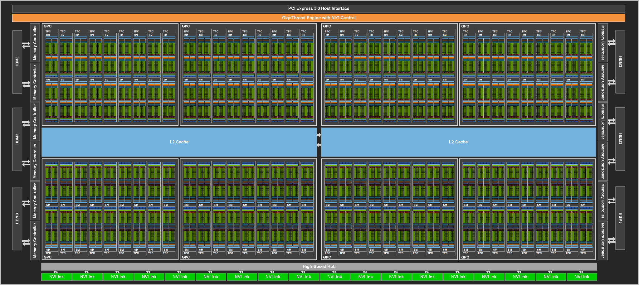
Like Nvidia’s previous compute GPUs, the Hopper/H100 will use HBM-type memory, with a 6144-bit bus for six packages of this die-stacked memory (this is unchanged from Ampere). The memory can be either HBM3 or HBM2e, the memory controllers seem to support both. Coupled with the memory subsystem is the L2 cache, which the chip has a total of 60 MB.
PCIe 5.0 and NVLink 4
In addition to these components, the GPU also has new connectivity. It supports PCI Express 5.0 as a first, but also NVLink 4. This interconnect has a bandwidth of 25 GB/s like NVLink 3, but the effective signal frequency is said to be 100 Gbps per pin instead of 50 Gbps, while the number of parallel lanes per NVLink interface has dropped from four to two.
The GH100 GPU has 18 of these interfaces, while the Ampere has only 12. Therefore, the bandwidth that NVLink can transfer when using all of them has increased by 50 %, from 600 GB/s for the Ampere GA100 to 900 GB/s for the GH100.
4 nm chip, 80 billion transistors
The entire GPU is a monolithic die – it’s made as a single silicon. So the GPU is not chiplet-based, as sometimes reported in preliminary leaks. The chip is 814 mm², which is roughly the same size as the 12 nm Volta/GV100 chip and smaller than the previous generation Ampere (GA100 is 826 mm²). It contains 80 billion transistors.
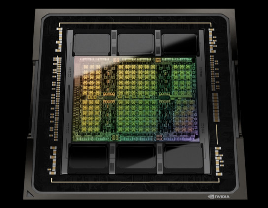
In the end, information that the chip could even be significantly larger than the so-called reticle limit turned out to be false. But there is also another surprise – Nvidia is not producing this GPU on the 5nm process, but on its improved derivative, the 4nm process. It’s TSMC technology, but the process is said to be customized for Nvidia, who calls it “4N” (this copies the designation they used for Samsung’s modified 8nm process, so it’s a bit confusing – TSMC calls their process backwards, N4).
Updated: The 4N manufacturing process is, according to leaker Kopite7kimi, possibly derived not from N4, but from the nominally 5nm N5P process. So Nvidia has renumbered its modified derivative a bit, but it’s probably not overly important, because both N4 and N5P are evolved variants of the same 5nm N5 process, just bent for different purposes. This may be why the information originally circulated that Hopper was a 5nm design. Yet the data stolen recently by hackers also seems to contain information about 5nm process node being used. It’s possible that the relabelling as “4N” may have come about after this hack, perhaps even in response to it.
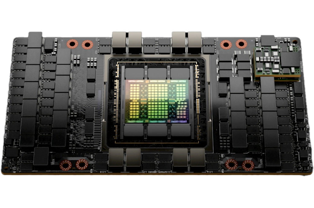
700W SXM version and PCIe version
Commercially sold models will have this GPU partially cut-down, as a few units need to be left off for redundancy. With a chip the size of the GH100, there will be relatively few silicon dies manufactured without any sort of manufacturing defect, so like consoles, it is expected from the start that part of the chip will be disabled in shipping products.
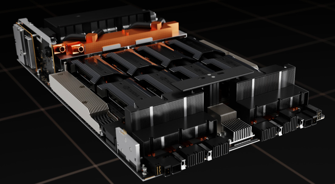
A more powerful of the variants the H100 accelerator will come in will be based on the proprietary SXM5 mezzanine format, which requires a special board and server. This version will have 132 active SM blocks (eight GPCs and 66 of the 72 TPCs), giving 16,896 shaders and 528 tensor cores. The frequency is expected to be somewhere around 1.78 GHz, but has not yet been finalized.
The GPU will use 80 GB of HBM3 memory, so again only five of the six stacks will be active, allowing Nvidia to reclaim even those manufactured GPUs where one of the HBM3 stacks has an error after completion. The memory bus is therefore only 5120 bits wide, which is also why the L2 cache is trimmed to 50MB.
The performance of this GPU is said to be up to 60 TFLOPS in FP64 precision calculations, but that’s with software tricks (using Tensor Core), the base FP64 performance is 30 TFLOPS (and 60 TFLOPS in FP32 single precision calculations). Tensor Core performance is claimed to be 500 TFLOPS in FP32 matrix calculations, 1000 TFLOPS in FP16 calculations, and FP8 format numbers are also supported, with performance up to 2000 TFLOPS – the same performance in the perhaps more practical INT8 integer format. This is just the pure physical computational performance of matrix operations, Nvidia quotes double that when using Structured Sparsity. Memory bandwidth is supposed to be up to 3 TB/s when using HBM3.
But this accelerator will also have a very high power draw. TDP has already reached 400 W in the last generation, and the Nvidia H100 continues the inflation – the TDP of the SXM5 model is 700 W! Cooling servers, where there will be maybe eight of these modules side by side, will be no simple task.
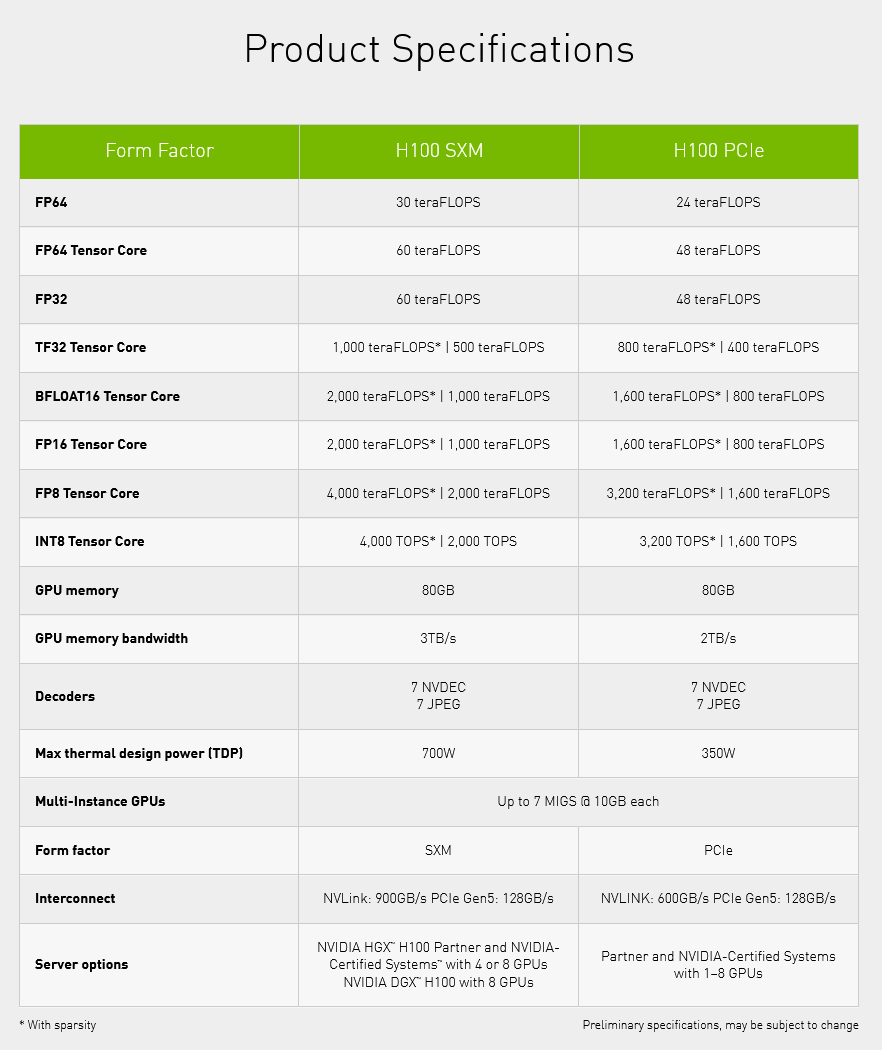
H100 as a PCIe 5.0 card will be 350W
There will also be a classic form-factor version in the form of a PCI Express 5.0 ×16 slot card. However, this model will have lower performance. The GPU will be trimmed down to just 14,592 shaders (114 SM) and 456 tensor cores. The memory will be kept at 80 GB, but older (and slower) HBM2e is to be used, so the total bandwidth will be only 2 TB/s. The bus here is therefore also 5120-bit with 50MB L2 cache. NVLink connectivity is somewhat limited, the card will probably only have 12 interfaces (so only 600 GB/s bandwidth). This card will have lower power draw, “only” 350W.
Nvidia lists performance to be at 80 % of the 700W SXM5 version – 24 TFLOPS in FP64 calculations and 400 TFLOPS in FP32 matrix calculations on tensor cores and so on (800 TFLOPS in FP16, 1600 TFLOPS in FP8/INT8).
Architectural inovations: Transformer Engine, Dynamic Programming
It has already been mentioned that Hopper supports calculations in the FP8 data format, i.e. floating point numbers with only 8-bit of total precision, whereas until now 8-bit numbers were used only in integer format (which has better practical precision but small range). Support for FP8 is part of a new tensor core architecture that Nvidia refers to as the “Transformer Engine”. This supports the transition to this reduced precision, increasing performance.
When training AI models, this reduced accuracy can be used in place of FP16 where it is feasible (Nvidia’s software should do this automatically). This should be useful for so-called transformer neural networks. Moreover, the FP8 support can then also be used directly for inference on the Hopper GPU, with AI networks that were trained using it.
The Hopper architecture also brings support for the so-called dynamic programming for the first time. This divides a task into smaller parts, whose partial results are then brought into the solution of the overall problem. This sub-division can allow for more optimal computation, as the processed subtask can be reused. The use of dynamic programming is enabled by the DPX instruction set extension, which is now making its debut in GPU Hopper.
Availability in the second half of the year
Although the Hopper has already been unveiled (on Tuesday), this is not yet a hard launch. Nvidia always announces these GPUs “on paper” in advance. The H100 accelerators are expected to start selling with actual physical availability in the third quarter of this year. They will be available in servers from various manufacturers, but also in servers made directly by Nvidia, which bases the HGX series servers on them.
Sources: Nvidia, AnandTech, VideoCardz
English translation and edit by Jozef Dudáš, original text by Jan Olšan, editor for Cnews.cz
⠀