First test of Zen 5 processor shows remarkable architectural features
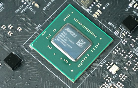
Next month, AMD will begin selling both mobile Ryzen AI 300 “Strix Point” processors with Zen 5 architecture and desktop Ryzen 9000 with this new core. AMD only said vague things about the core at Computex, mentioning a 16% increase in IPC (for selected programs, of course), but now a test of a an actual specimen has appeared on the internet, revealing more about the Zen 5 architecture. And it’s very interesting stuff.
This test is originally in Chinese and was posted by David Huang, who got his hands on a laptop with a Ryzen AI 9 365 processor, on his blog. According to his disclaimer, the processor might not necessarily perform as well as a final retail hardware should as the firmware might not be final. However, significant insight into architectural features can be gleaned from the testing.
The Ryzen 9 AI 365 is designed for laptops, so it’s a Strix Point APU, with it being the second model in the series. It carries four Zen 5 cores with a maximum clock speed of 5.0GHz (the top model has a slightly higher boost of 5.1GHz), which are organised in a single CCX block with a shared 16MB L3 cache.
Additionally, the Strix Point APU has eight Zen 5c cores in a second, separate CCX block with 8MB of L3 cache. Their maximum clock speed appears to be 4.0GHz (in the 365 model), although they are more likely to run somewhere around 3.7GHz in multi-threaded tasks.
Unfortunately, this means there is not one shared L3 cache shared by all 12 cores, which the CPU could fully use even in a single-threaded task. The Ryzen AI 9 365 that was tested has the Zen 5c core count cut to 6 from 8, so it is a 10-core with 20 threads. The tested laptop was equipped with 32GB of LPDDR5X-7500 memory and had a TDP set at 54W.
Increases in performance per 1 MHz for the mobile Zen 5 sample
First up, information about the measured IPC (i.e. performance per 1 MHz of core clock speed), although that is actually the part about this teste that should be taken with the biggest grain of salt – as already mentioned, the performance may not yet match the final product. Huang measured the single-threaded improvement in IPC in SPEC CPU 2017 (more precisely in the integer part, SPECint rate-1) and came up with a +9.71% improvement for Zen 5 over Zen 4. It looks similarly for Zen 5c, where we even see a slightly higher increase, but this is likely just distortion due to the lower clock speed and the IPC is really equal. The biggest improvement, 24%, is in the 500.perlbench_r subtest, in which previous AMD architectures did relatively worse, and Zen 5 can be said to simply be catching up. On the other hand, 531.deep-sjeng_r has an IPC reduction of 5%.
Geekbench 6 signals a better improvement in IPC, showing +15,28 % (15.13% for integer, 15.54% for floating point subtests). Geekbench 5 similarly shows an IPC improvement of +17,66 % (17.26% for integer, 19.02% for floating point subtests). All these tests are performed under Linux (Debian sid). The preliminary single-threaded scores for this Ryzen AI 365 sample, by the way, came out to 2995 points in Geekbench 6 and 2286 in Geekbench 5. The multi-threaded scores were 14,530 and 13,926 points respectivelly (recall that this is a cut down 10-core model, and the single-threaded test should also be about a few dozen points better for the 12-core HX 370 model due to the extra 100 MHz).

Architectural features
What did David Huang find out about the core’s inner working? Microbenchmarking apparently confirms that there are added ALUs in the core, however Zen 5 introduces some regressions as well. For example, the integer SIMD addition has had its latency increased from one cycle to two, this applies to both SSEx, AVX2 and AVX-512 instructions. Presumably this is done to achieve better clock speeds, but it can theoretically reduce performance when frequent data dependencies are involved.
The core has a reduced uOP cache according to the measurements, which is a cache that stores already decoded instructions. While in Zen 4 it had a capacity of 6750 entries, Zen 5 apparently reverted to the 4096 entry capacity of Zen 2 and 3 (theoretically, this could also be because the core was partially developed in parallel with Zen 4, not being strictly based on it but instead branching of from earlier state of AMD’s development tree).
Instead of investing into uOP cache, Zen 5 has added instruction decoders, of which there are eight, but split into two clusters. The core can also fetch a sequence of program instructions from two L1 instruction cache locations at the same time, so that the two clusters of decoders can operate simultaneously. And it is also able to fetch two separate instruction (operation) streams from the uOP cache in a similar way.
The Zen 5 core handles branching better. For branches not taken (the execution does not result in jump to another code point), it can process three branches per cycle instead of two. What is more notable however, it can process two taken branches per cycle, which is the harder case of branches that do end up with a jump. This is a significant improvement, presumably made possible by those doubled decoders.

Zen 5 has a 48KB L1 data cache with a latency of 4 cycles, a 50% increase in capacity over previous cores, while maintaining the same latency. Intel has the same capacity for big cores (but Sunny Cove and Golden Cove had a latency of 5 cycles, Lion Cove, where it is referred to as the L0 cache, also has 48 KB with a latency of 4 cycles). The L2 cache has the same capacity of 1 MB and latency of 14 cycles as Zen 4 (previous Zen cores had 512KB L2 cache with latency of 12 cycles). The L3 cache seems to have improved latency from 50 to 46 cycles, but it’s possible this doesn’t translate to the desktop version of Zen 5 with its higher L3 capacity, its latency might be higher.
Beware, Zen 5 in laptops and Zen 5 in desktops will probably be quite different
An important observation is that the Zen 5 core used in Ryzen AI 300 may differ from desktop and server Zen 5. There appears to be no difference in IPC (that is, if we ignore the impact of the smaller L3 cache block with Zen 5c cores) or instruction support between the big or classic Zen 5 and the “dense” Zen 5c. Zen 5c even supports AVX-512 instructions and has the same natively 512-bit wide SIMD units, as well as support for all instructions.
Ironically, there could instead be a difference in how the big core in the mobile Ryzen AI 300 (Strix Point) looks versus the standard version of the core in desktops and servers. According to David Huang’s microbenchmarking, AMD has apparently chopped the SIMD (FPU) unit of both the Zen 5c and Zen 5 cores in the Strix Point chip to half the pipeline count. This cuts the theoretical compute performance in 128-bit SSEx and 256-bit AVX/AVX2 operations in half, the core can only process half of them per cycle compared to Zen 4.
However, these pipelines retain 512-bit width (even for dense Zen 5c cores). So there is one way to get the same SIMD performance out of this core as out of Zen 4 – by using 512-bit AVX-512 vectors. This is because the core processes these in a single pass, whereas Zen 4 with its 256-bit units performs them in two halves twice over. Thus, even in this cut-down version, Zen 5 can have the same performance (in theory at least) as Zen 4, when running optimal AVX-512 code. Performance will probably suffer by some percent when using smaller vector instructions, however.
This sounds similar to the thing AMD did with the Zen 2 “Lite” cores used in the PlayStation 5 (and presumably also in the Mendocino APU, the Ryzen 7020U). According to benchmarks done on the PS5 SoC, apparently such a stripped-down SIMD unit may not be such a blow to performance in a large number of applications, including games, as the Chips and Cheese website tests show. In Zen 2 “Lite” AMD left the capacity of the FPU queues the same as in the full-fledged version, which masks the differences in the backend execution performance of SIMD operations to a good degree. Hopefully, AMD will be similarly successful at keeping the performance relatively good with this Zen 5 variant too.
Full-fledged SIMD unit only in desktop?
However, it looks likely that this only applies to the mobile version. For now, we can probably expect the desktop Zen 5 in Ryzen 9000 to have the pipeline count untouched, so it will retain the same performance in SSEx and AVX/AVX2 operations, but achieve double in AVX-512 instructions. It’s a conjecture that hasn’t been confirmed yet, but it wouldn’t make much sense otherwise.
So it looks like AMD will start making more differences between the mobile and desktop-server versions of the core. Up until now, the architecture was the same and it was only the memory controller and L3 cache capacity where the implementations differed (this in itself may have been reducing the IPC of mobile Ryzen cores down a bit, even in the past). Apparently the changes will be more profound from now on. Therefore, it is possible that Zen 5 in AI 300 Ryzens will have a slightly lower IPC than Zen 5 in Ryzen 9000 (and Epyc 9005).
This architectural difference is likely to have noticeable impacts on the performance of software encoding and similar software multimedia processing on laptops. In most applications, however, the performance drop will be much less than the theoretical -50% impact. The biggest problema could probably be in HPC and scientific computing type code if it only uses AVX and SSEx instructions. However, such code probably has the best chance that AVX-512 is applicable to it. If you run such tasks, the solution could be the upcoming powerful Strix Halo mobile processors, which have 16 Zen 5 cores that will probably use the full-fat desktop architecture, i.e. without the SIMD unit being cut-down.

Exactly what the effects of this cut down SIMD / FPU will look like and how much better Zen 5 will be on desktop as a result, we will only see after the release of reviews and especially as there is deeper analysis done over time. For now, it’s probably premature to judge how much of a compromise this will be.
Dual decoders – an echo of Bulldozer (Steamroller)?
Apart from this controversial feature (hopefully only concerning the mobile version) there is one more very interesting thing. David Huang’s test confirmed that Zen 5 has decoders divided into two clusters of four, as mentioned above. Previous AMD cores had four decoders, so this is and also is not a doubling. Architecturally, it’s apparently quite similar to the dual decoders of the Intel Atom line of cores – Tremont and Gracemont, which have a two three-wide decoder clusters (the new Skymont even has three such clusters). However, this is not equivalent to a core that has eight decoders in a single cluster (like Intel Lion Cove) and is able to employ all eight in a single thread.
- Read more: Skymont architecture analysed: Intel little core outgrows the big?
- Read more: Intel’s new P-Core: Lion Cove is the biggest change since Nehalem
Zen 5 doesn’t seem to be able to do this, or at least not in a completely trivial sequential code with absence of branching. According to David Huang, when testing a series of NOPs, it turns out that in linear code, Zen 5 can run at most four x86 instructions per cycle in a single thread through the decoders, so it can only employ a single cluster (which means it’s on par with Zen 1 to 4). However, the core can process more if it takes instructions from the uOP cache instead.
However, if there is a branch in the code and the program jumps to a different address, then the second decoder cluster can probably step in and join, given the ability of the fetch to load instructions from two cache locations at the same time. In this case, the first cluster will decode the code up to and including the branching instruction, and the second cluster will start decoding immediately where the code jumps to, since that address is always the beginning of an x86instruction. This therefore circumvents the problem of the x86 architecture having variable instruction lengths, which makes it not possible to trivially know in advance where instructions start as in the ARM architecture with constant instruction lengths (where this clustering scheme would not be necessary and decoders are easier to parallelize in a single cluster).
That means the second cluster of decoders helps less often, but it is possible that it still adds relatively enough IPC since branching should be present frequently in code. It has been often cited that, on average, there may be up to one branch for every six instructions of code, but of course this will depend a lot on the type of program you use as the reference. However, if such heavily branched code is frequent, then Zen 5 may benefit from its two clusters frequently even in single-thread tasks, much like Intel’s E-cores. The latter, however, may have the ability to involve multiple clusters of decoders more often because they use instruction pre-decoding, which figures out where instructions start in advance, making it easy for the other decoder clusters to pick up work in paralel to the first.

David Huang is theorising that in the future AMD could also switch to such a pre-decoding system instead of using the uOP cache, and its cores could work similarly to Intel’s “mont” cores. But this is just a hypothesis, it’s hard to know for sure at this moment. How often Zen 5 in its current form can utilise the second cluster of decoders in single-thread tasks will need to be analyzed further.
However, all this applies to running single-threaded code on the core. But the situation changes a lot if the Zen 5 core engages SMT and handles two threads. David Huang has verified that in this case it actually decodes up to eight instructions per cycle. What happens is that each of the threads gets a dedicated cluster, so while the rest of the resources in the core are shared, the threads have dedicated decoders. This should help multithreaded CPU performance (in a situation where both threads on the cores are under load). Thus, Zen 5 could deliver a larger percentage of performance improvement per 1 MHz in multi-threaded applications than in single-threaded ones.
There is an interesting historical parallel with the development of AMD’s previous and not entirely successful family of CPU architectures, the Bulldozer (“construction machines family”) line of cores – but especially with its later derivatives. With Bulldozer, AMD used a module consisting of two cores with a high degree of integration between them and some parts shared. For example, the FPU was shared completely and acted even then as a single core with SMT. The cores had separate integer and AGU units, but the cluster of decoders (also four-wide) was one of the parts the cores shared.
But after the first two architectures (Bulldozer and Piledriver), AMD made a compromise in the Steamroller architecture and gave a separate dedicated decoder to both cores. Thus, in a broad sense (and merely in this particular detail), Zen 5 kind of repeats the Steamroller approach. However, in Steamroller, one core could not benefit from the second cluster of decoders in a single-threaded task, which is hopefully possible in Zen 5 (in that taken-branch scenarios).

Nice synergy with SMT
This concept looks like a potentially successful element. Interestingly, while Intel is betting less on SMT now, preferring to simplify the core for mobile and desktop processors in the hope that this will make it easier to improve single-threaded performance, AMD seems to be putting more emphasis on SMT with Zen 5 than before. At least on the surface of it, this is how one can interpret the fact that the core has dual decoders, the full performance of which it can only use when SMT is used and two threads are running on it.
However, the neat thing about this is that, unlike Steamroller, it’s not actually adding resources purely for the sake of SMT. Intel, after all, uses the same doubled or even tripled decoder clusters in E-Cores precisely as a means to improve single-threaded performance purely, not exploiting it for the potential improvement for multi-threaded workloads at all.
The SMT technique is conceptually interesting exactly because in some ways it does not force CPU architects to choose between single-threaded and multi-threaded performance, since the same resources in a single core can contribute in both disciplines. Cores with high IPC and single-threaded performance achieved through a large number of execution units and resources typically rarely utilise all of their resources at once due to limits faced in parallel out-of-order instruction processing. SMT, when processing two threads, allows to “recuperate” part of the unused execution resources. However, the performance when using SMT on such cores directly benefits from the architects having added those resources in order to increase the single-threaded performance, so the two goals are in symbiosis and with a little luck the architect can successfully play both sides.
If AMD wanted to improve multi-threaded performance by duplicating some structures so that each thread has its own dedicated set of these resources, it goes against this idea because these extra resources will not be usable when running a single-threaded task. However, here in the case of the doubled decoders, it seems they have managed to use these doubled resources in both single-threaded mode (which is the difference against Steamroller) and SMT mode (the difference against Intel’s E-Cores) at the same time, which seems like a very elegant and efficient idea on paper, exactly in line with that SMT concept where newly added and improved core resources target to improve single-threaded as well as multi-threaded performance in unison.
However, we don’t know yet that AMD isn’t paying some high price in power consumption, die area or complexity for this feature, so at this moment we can’t know for sure if this solution really works well in practice. Sometimes a seemingly elegant idea has to be abandoned for reasons like this, because more primitive and less clever approaches may end up producing more efficient results when it all comes together.
These tests have produced some interesting findings, but as already mentioned, they should be seen as preliminary. Particularly don’t take the data on percentage improvements in IPC as definitive yet, tempting as that is. Once more reviews come out (and tests of the desktop version are available), it will hopefully be easier to assess how much of an improvement Zen 5 is over Zen 4, and how advantageous or disadvantageous are the compromises that these preliminary tests suggest have been made to the mobile version of the core.
Source: David Huang
English translation and edit by Jozef Dudáš
⠀


